IN2FAB joins the SemiWiki community

IN2FAB Joins SemiWiki.com to Promote Semiconductor IP Migration Services
Northampton, UK — September 16, 2026 — IN2FAB, a provider of semiconductor circuit porting, migration, and security solutions, today announced that it has joined the SemiWiki community to provide semiconductor companies detailed information about to its IP migration expertise and services.
As semiconductor companies increasingly face the challenge of moving established IP to new process nodes, foundries, and design environments, preserving existing intellectual property while reducing redesign time and risk has become increasingly important. IN2FAB provides specialized migration technology and engineering services for analog, mixed-signal, and digital IP.
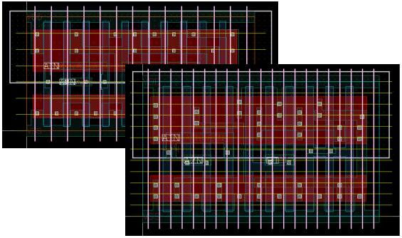
IN2FAB's OSIRIS Migration technology operates within Cadence Virtuoso and is designed to migrate both schematic and physical layout while preserving the original circuit hierarchy and physical design structure. Unlike approaches that primarily regenerate a schematic and then require the layout to be redesigned, OSIRIS directly translates the existing layout to the target process, including PDK-dependent elements such as devices, PCells, vias, and layout rules.
“There is a tremendous amount of valuable semiconductor IP embedded in existing designs but moving that IP to a new process can traditionally require significant engineering effort,” said Tim Regan, CEO of IN2FAB. “Our goal is to make migration a practical alternative to starting over. Joining the SemiWiki community gives us an opportunity to reach semiconductor engineering teams and share what we have learned from years of real-world IP migration.”
"I have seen the challenges of process migration up close. These are very difficult problems to solve and IN2FAB is providing effective solutions across many markets and customers." Daniel Nenni, Founder SemiWiki.com
"I've faced design re-targeting challenges many times in my career. IN2FAB delivers a reliable and robust approach that delivers considerable value." Mike Gianfanga. SemiWiki blogger and industry consultant
IN2FAB's migration services support projects ranging from individual IP blocks to larger collections of analog, mixed-signal, and digital circuits. Customers can engage IN2FAB for migration engineering services or use OSIRIS technology under license, depending on their requirements.
The company has developed migration flows supporting multiple process technologies, foundries, and design environments. Its experience includes migration projects for semiconductor companies ranging from specialized IP providers to large semiconductor manufacturers.
IN2FAB is also expanding its migration technology with new capabilities for digital and AI-assisted semiconductor design migration. The company's broader technology roadmap is focused on reducing the engineering effort required to modernize and reuse existing semiconductor IP.
About IN2FAB
IN2FAB is a semiconductor technology company specializing in circuit porting, IP migration, and semiconductor security. Its OSIRIS Migration platform provides automated migration of semiconductor schematics and physical layouts between process technologies while maintaining design structure. IN2FAB also develops Secure PDK technology for protecting semiconductor design assets and PDK intellectual property.
For more information about IN2FAB and its semiconductor IP migration services, visit IN2FAB on SemiWiki.com or contact IN2FAB directly on its website at https://www.in2fab.com.
About SemiWiki
SemiWiki is an Open Forum for Semiconductor professionals with more than 350,000 registered members that publishes industry news, analysis, technical articles, webinars, podcasts, videos, and forum discussions.
Media Contact:
IN2FAB Technology
Northampton
United Kingdom
Bronte Hobson-Scott
media@in2fab.com