For semiconductor companies, analog IP migration is increasingly becoming a business decision rather than simply a technical exercise. The faster a company can move proven analog designs between process nodes or foundries, the faster it can reach validated silicon, reduce engineering cost, and respond to market opportunities.
In analog design, the critical milestone is not schematic completion—it is reaching
post-layout simulation with extracted parasitics (PEX). This is where real circuit behavior is verified and where issues such as coupling, matching degradation, and parasitic effects become visible.
Traditional schematic migration approaches delay this point significantly. The process typically involves schematic conversion, device resizing, re-validation, complete layout recreation, extraction, and multiple optimization loops. While schematic resizing tools can assist with small to medium analog blocks, they do not scale effectively to large mixed-signal systems such as SerDes or Bluetooth designs, where layout interaction dominates performance. In practice, these large designs still require substantial manual redesign and re-layout effort.
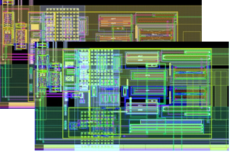
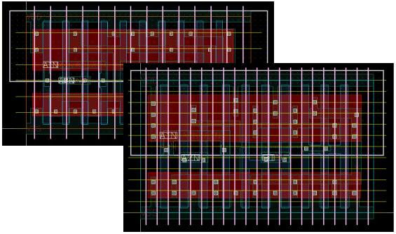
Direct layout migration changes the model entirely by preserving the original layout intent, including placement, symmetry, routing topology, and matching structures. This allows teams to reach extracted simulation dramatically faster and begin validating real performance much earlier in the project cycle.
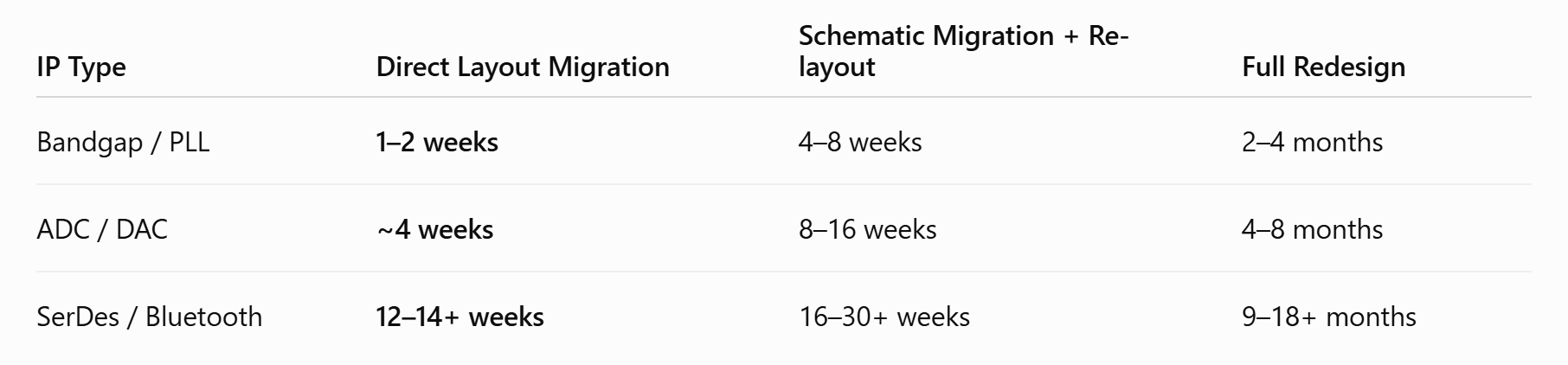
The migration times shown below are not theoretical estimates—they are based on actual customer migration projects completed by IN2FAB's engineers across a range of analog and mixed-signal IP. These projects span everything from relatively compact analog building blocks, such as bandgaps and PLLs, to complex data converters and large high-speed interfaces. While every migration project has its own challenges and the exact schedule depends on the source and target technologies, the figures represent typical delivery times achieved using direct layout migration on production-quality customer designs. They demonstrate what is possible when proven layout IP is migrated rather than recreated from a modified schematic.
The schedule difference is more than an engineering metric—it directly affects business outcomes. Even for highly complex systems such as SerDes and wireless transceivers, direct layout migration can reduce development time from many months to approximately three months, allowing engineering teams to begin post-layout validation far sooner. Earlier access to extracted simulation reduces project risk, shortens design iterations, and accelerates the path to tapeout and revenue.
As analog and mixed-signal designs continue to grow in complexity, the ability to migrate proven IP quickly is becoming a significant competitive advantage. Direct layout migration enables companies to shorten development schedules, reduce engineering costs, and reach validated silicon months sooner than traditional migration or redesign approaches. Whether you are planning a foundry transition, moving to a more advanced process node, or extending the life of an existing IP portfolio, rapid layout migration can help you achieve your goals with less risk, lower cost and greater predictability. If you are evaluating your next migration project, we'd be pleased to discuss your requirements, review your existing IP, and show how our proven layout migration technology can accelerate your path to silicon.