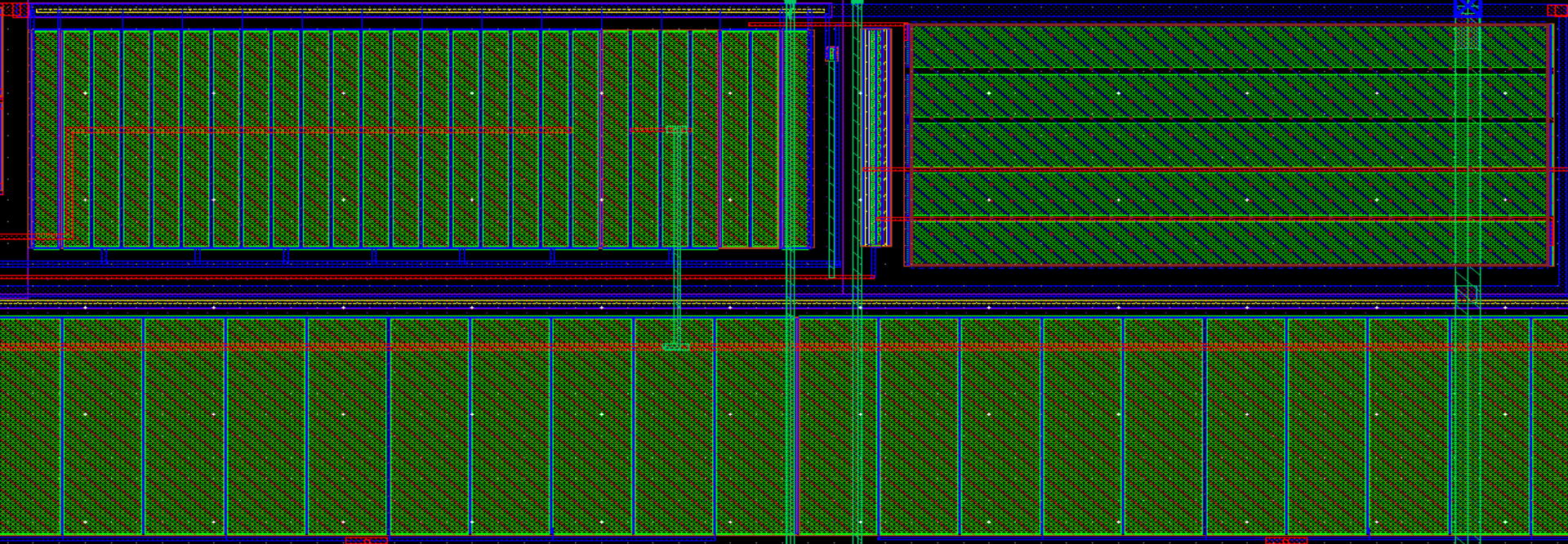
A mature layout contains far more knowledge than the schematic captures. Device placement, orientation, matching structures, routing topology, and parasitic balancing are the result of engineering judgment and silicon learning. While the schematic describes circuit function, product success is often encoded in the layout. Direct migration preserves this physical intelligence, whereas schematic regeneration frequently loses subtle but performance-critical details.
Parasitics are another decisive factor. Analog and RF designs rely on carefully balanced wiring, coupling, and symmetry that exist only in the physical implementation. Regenerating layout from a schematic may produce a functionally correct circuit, but not a performance-equivalent one. Migrating the layout enables early extraction in the new process, allowing designers to tune the circuit with real parasitic data and move toward signoff with confidence.
Direct layout migration also reflects the reality of IP porting. While EDA demos start from pristine databases, real-world IP often includes missing constraints, outdated schematics, mismatched hierarchy, or hand-crafted geometry that was never meant to be rebuilt. Layout migration works from whatever exists today, and remains the fastest path to silicon in a new process or foundry.


