Blog Layout

Migrating and Modifying Standard Cell Libraries

Automated modifications to standard cell libraries saves time and money

Predefined logic functions in standard cells lie at the heart of digital circuit design.  These components form the bedrock in digital circuits, where powerful place & route tools use them to build circuits that drive the electronics revolution. 


Developing and validating a new standard cell library for a new technology node can be expensive due to the investment required in design, and verification efforts. Companies must weigh the cost of updating the standard cell library against the benefits gained from utilizing the new technology node.  Depending on the resources available, updating a standard cell library to a new technology node may require significant time, manpower, and computational resources. Balancing these constraints while meeting project deadlines and quality goals can be a challenge.


In addition to layer and gate size changes, each process node comes with its own set of design rules governing minimum feature sizes, spacing, and other layout constraints.  Engineers must also choose optimum cell height and routing pitch to delivery maximum area and routing density.  The complexity of these constraints prevents designers from running tests to find the optimum values for the new technology.


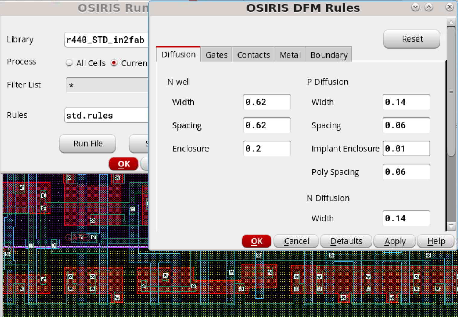
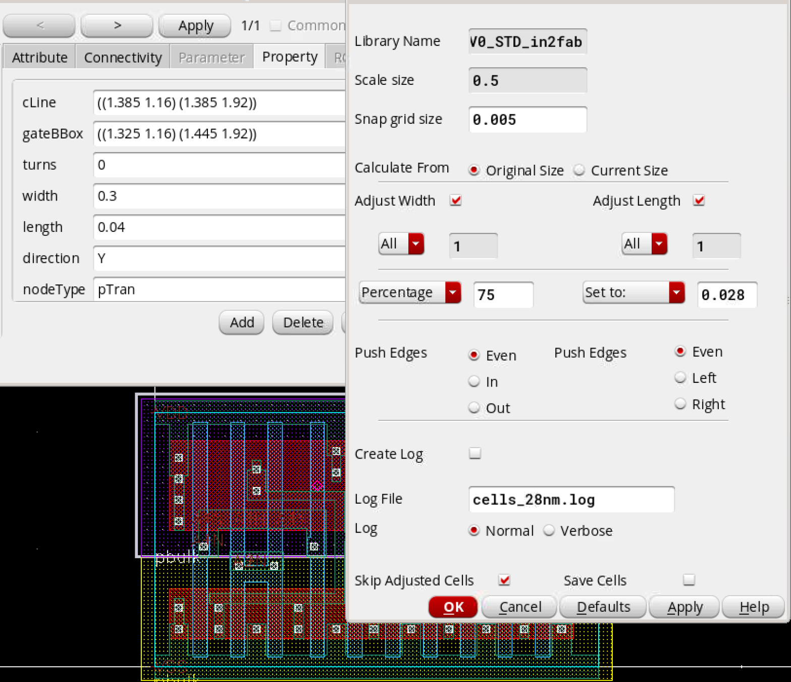
Unlike analog layout based on parameterized cells, standard cells are usually constructed of polygons that make up the devices and interconnect.  By identifying the elements of the layout that make up the transistors, the standard cell migration technology can update gate dimensions, then adjust the rest of the layout to meet design rules.


IN2FAB's standard cell migration technology can process hundreds of cells in a matter of minutes, to move them to a new technology or simply apply new rules.  Schematics for each cell are updated to contain new symbols and parameters, while the layout is converted to match the new manufacturing process requirements and rules.


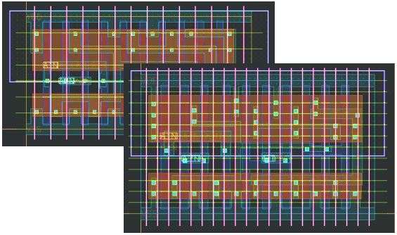
By adopting this approach, cell libraries maintain their structure and device positioning, while the shapes for each device are adjusted to match new design rules.

OSIRIS standard cells uses a powerful compaction engine on the back end of the process to enforce design rule compliance and boundary positioning.  Well, implant and diffusion shapes are set to a standard height, while individual circuit elements are moved to meet DRC rules.  


More complex design rules such as DFM or updated pin grids are also enforced, to ensure maximum density and routability.  Specific area requirements for via landing points can also be applied, moving metal shapes to the specified grid as required. 

The rapid processing times for entire libraries mean that designers can adjust parameters and run tests in a matter of minutes.  Cell sizes and routing grids can be adjusted to evaluate their impact across the entire cell library, while detailed information such as DFM rules can be factored in to the process as required. 


Efficient standard cell migration combined with grid adjustment and DFM integration allows engineers to evaluate and test new technologies with minimum effort.  This ensures companies can protect and leverage their standard cell IP for years to come. 

13 Dec, 2023
Rapid porting accelerates SoC development using existing cores or 3rd party IP.
by VF1935 16 Aug, 2023
IN2FAB to add DFM capability to OSIRIS tools with support from Innovate UK
25 Jun, 2023
Database translation tools enable rapid circuit integration
19 Apr, 2023
Migrating standard cells pays huge dividends
19 Apr, 2023
Should a migration project be performed internally or through a design service?
by VF1935 19 Apr, 2023
Migration from planar silicon to GF 22FDX SOI process
Share by: