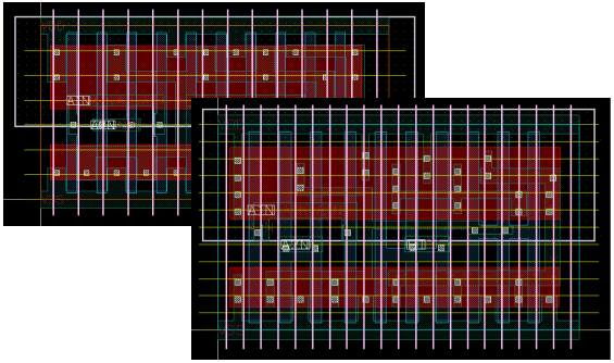
A migration feasibility study can turn an uncertain redesign into a measurable engineering project
Moving semiconductor IP to a new process technology is usually treated as a redesign problem, but what if much of the original design could be reused?
For analog and mixed-signal IP, years of engineering effort are embedded not only in the schematic, but also in the physical layout. Device sizing, matching, symmetry, routing, shielding, placement, hierarchy, and other physical design decisions can represent a substantial investment.
Starting again from a schematic can mean throwing away much of that investment but IN2FAB takes a different approach.
Our migration technology and engineering services are designed to determine how much of an existing design can be preserved and migrated to a new technology—before a customer commits to a full redesign or migration program. That is where an
IN2FAB Migration Feasibility Study can provide significant value.
Don't estimate your migration. Test it.
The biggest question facing a company considering IP migration is often deceptively simple:
Can our existing IP be migrated economically to the target process?
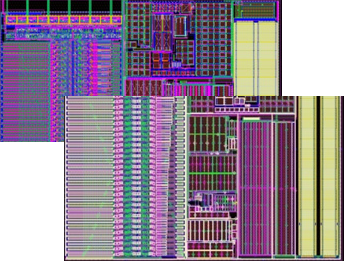
Comparison between the foundries and process nodes are a key part of the equation, but much of the answer depends on the actual design. Generic discussions about migration capabilities cannot tell you how your particular IP will behave. Every design has its own devices, layout structures, PCells, vias, design-rule dependencies, and technology-specific implementation choices. An IN2FAB feasibility study applies our migration technology to a representative portion of your actual IP. Instead of estimating what migration might require, you get an opportunity to see what migration can actually accomplish.
See your design in the target technology
You can see:
- How devices map to the target process
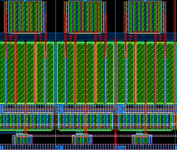
- How physical structures translate
- How devices and parameters are translated and highlight limits in device sizes
- Which portions of the layout can be preserved
- Where design-rule differences create challenges
- Which structures require engineering intervention
- What level of redesign may be necessary
The result is a much more concrete picture of the migration project to inform both technical and business decisions.
Discover the value hidden in your existing IP
Many semiconductor companies have large portfolios of proven IP developed over years or even decades. That IP may represent millions of dollars of engineering investment. When a company moves to a new process, the conventional response can be to redesign significant portions of that IP. But a redesign is not necessarily the only option.
But a redesign is not necessarily the only option. If existing layouts can be migrated and reused, companies may be able to reduce the amount of new design work required while retaining valuable knowledge already embedded in the original implementation.
Migration can turn existing IP into an asset for the next process generation instead of treating it as obsolete.
A feasibility study provides a way to determine whether that opportunity exists.
Reduce risk before committing engineering resources
A full migration program can require substantial engineering resources. Before making that commitment, companies need answers to practical questions:
- How much work will migration require?
- Which parts can be automated?
- Where will engineers need to intervene?
- What are the major technical risks?
- How long could the migration take?
- Is migration more attractive than redesign?
An IN2FAB feasibility study is designed to answer these questions early. Rather than committing immediately to a large migration project, you can start with a focused evaluation and use the results to define the next step.
Find out where automation delivers the most value
Turn an unknown project into a structured migration plan
One of the most valuable outputs of a feasibility study is a better-defined project. The results can provide the basis for:
- Migration effort visibility
- Engineering resource requirements
- Project schedules
- Technical assessment and component details
- Automation opportunities
- Verification requirements
- Migration priorities across an IP portfolio
Instead of beginning a migration with a broad estimate, you can begin with information derived from the actual design. That can make the difference between an open-ended engineering project and a defined migration program. You don't need to commit your entire IP portfolio to find out whether migration is viable. IN2FAB can use that design to evaluate the migration path and demonstrate the technology, giving the foundation for a broader migration program.
Migration technology or migration services? Or both?
Is your IP ready for its next process?
If you have proven analog, mixed-signal, or other custom IP that needs to move to a new technology, IN2FAB can evaluate the migration opportunity using your actual design. Whether it's a pilot block, an IP licensing opportunity or porting a complete IP platform, a migration feasibility study delivers a clear picture of technical detail, schedule and cost.
Contact IN2FAB to discuss a Migration Feasibility Study and find out how much of your existing IP can be reused.
Don't automatically redesign what you may be able to migrate.