Migration Service Examples
IN2FAB's design service group has migrated hundreds of circuits to new foundries and process nodes. From analog and digital library IP, to the biggest IP blocks, circuits are ported to a new technology in a matter of weeks.

Analog IP Platform
Migration of multiple modules in a core analog IP platform to a new foundries and process nodes. The IP portfolio included PLLs, bandgaps, ADCs and DACs and each module was checked and delivered in the new technology.
The migrated circuits accelerated the customer's move to new process nodes across three separate foundries, allowing them to reduce costs and secure second source manufacturing. IN2FAB's migration services helped them to meet their goals far in advance of standard product design and redevelopment.
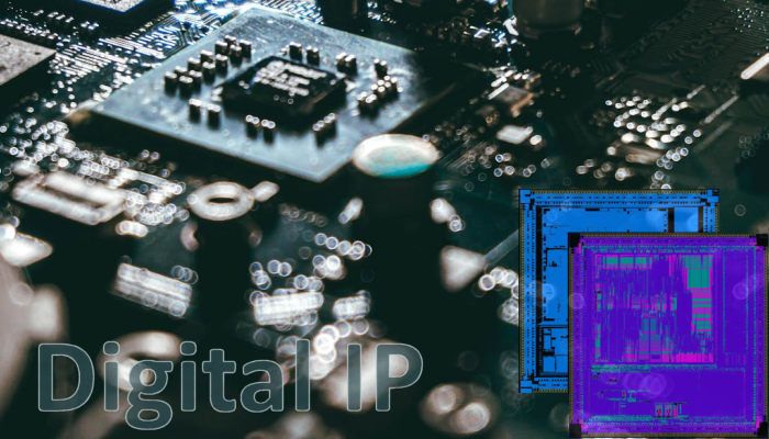
Wifi IP Core
Full migration of schematics and layout of a wireless IP cores including analog circuitry and on-chip radios for modular Wi-Fi. This migration was part of a multiple projects to translate communications devices which also included a full Bluetooth core. The circuits were translated between two major foundries and allowed the customer to expand their IP portfolio and take advantage of new licensing opportunities.
Source design databases were based on the Cadence Virtuoso™ platform and included Parameterized cells, multi-part paths and fluid guard rings along with netlist driven layout data. These were maintained in the migrated database to ensure easy editing in the future.


High Performance IO Cores
Full migration of the schematic, layout and associated data for an advanced HDMI core from a flagship European electronics company which was used in the support of several multimedia SoC projects. IN2FAB's design migration services allowed the IP vendor to rapidly accelerate their produce development in a competitive market and retain their own design engineers for other projects.
The fully migrated design was delivered just seven weeks after the project started and became a key element in the customer's multimedia platform.
MIPI IP Core
Migration of schematics and layout for a MIPI DPHY core to support a series of SoC products. The circuits were migrated from an internal foundry based on custom built design kits to a large commercial manufacturer. All elements in the design kit were mapped to the customer foundry's technology and the full design migrated and delivered in six weeks.


Standard Cell Library
Adjust an 800 element standard cell library to use a smaller routing grid while increasing pin locations and contact coverage. The entire project was completed in three weeks which included data preparation and cell modification. Cell abutment was checked through all placement orientations and positions, and extra test cells were generated to allow the customer to automatically run future DRC and LVS checks in batches.
The new library enabled a routing density increase of approximately 1.5x without increasing cell sizes.
Microprocessor SoC
Full microprocessor chip, including CPU, cache, north and south bridge, I/O and ESD structures. The entire chip was migrated from a foundry that was closing to a new foundry to continue production to serve a large customer base. The complete chip was translated to the new foundry and design rules along with legacy design files and other data.
The entire chip, including schematic, netlist and layout was converted in six weeks and booted to operation on receipt of first silicon. The chip is now in high-volume production.