Migration To GlobalFoundries 22FDX SOI

IN2FAB Technology joined Global Foundries’ FDXcelerator™ program to help companies move their IP to 22FDX.  IN2FAB's advanced design migration technology transfers planar circuits to 22FDX® in a fraction of the time and cost taken for a redesign.

Global Foundries has invested heavily in new technologies including a range of Silicon on Insulator (SOI) processes for advanced SoCs. This process is ideal for devices that must combine high performance with extremely low power consumption but without the high cost of FinFET manufacturing. 


Migrating circuits to an SOI process presents extra challenges that are not found in bulk silicon technology.  Devices can adjusted to take advantage of the benefits of body biasing and other factors like layer coloring, dummy shapes and layout dependent effects as well as complex changes in device construction and rules must also be addressed. 

An alternative to full redesign comes in the form of analog and mixed signal circuit migration.  This involves translating existing circuits to use elements from a new process design kit (PDK) and adapt to the new rules and requirements of the target foundry.  The structure, hierarchy and architecture remain the same as the original so most of the source data is reused directly with adjustments to suit the new technology.  Schematic circuits can be made available for simulation in a very short time so decisions made about functionality and circuit enhancements.  Once the circuit is validated in this way the full migration can be performed to deliver a completed layout that meets the needs of the target foundry.

Schematic Migration and Simulation

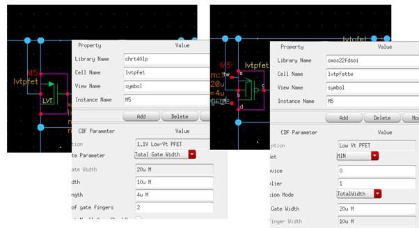
Schematic and layout data are translated through map files that describe the old and new circuit elements along with pin and parameter information.  Core circuit components will be replaced with equivalent devices from the new PDK and any standard cells placed in the analog hierarchy should also be swapped to elements from a library in the new process. 


Physical information including symbols, wires and pins are migrated and adapted to suit the new PDK, with automatic position adjustment, rewiring, short location and connectivity checking tools.  Some SOI transistors have extra pins for body biasing so these can be connected as required.  Automatic short location within the migration tools picks up any places where a new pin shorts to an existing wire and re-routes to fix the problem.


Parameter limits play an important part in process migration and tools must recognise instances that must change in the target process due to limits in maximum or minimum values and adapt them accordingly.  Similar changes are often required in passive components where new sizes or number of segments are required.  OSIRIS migration tools calculate the values automatically so there is no need for engineers to calculate conversion factors.


Once the schematic migration is complete and the test benches are converted, the circuit can run through first level simulation.  This should confirm overall functionality of the system in the new process as the simulation is using models from the 22FDX® libraries.


A migrated schematic means that designers can get to the circuit tuning level without having to worry about building an entirely new design from scratch.  Once this migration flow is configured, even large designs can be migrated and ready for simulation in a matter of hours.

Layout Migration

Layout migration is much more complex than translating schematics and moving from bulk silicon to an SOI process presents some extra challenges.  However, a comprehensive migration flow will address the intricacies of the different circuit elements while giving designers control and flexibility to update the circuits where necessary.  While schematic migration is fully automated, some sort of interaction is usually necessary during layout migration to adapt the design where necessary.


The key to migrating analog layout is to use foundry elements from the target PDK to build the migrated design.  Parameterised cells (Pcells), vias and shape based data from the original circuit are replaced by elements from the new PDK through the hierarchy with component parameters adapted as required.  A shape based flow that reduces the design to a collection of polygons will never be able to convert bulk silicon layout to SOI but using Pcells means that devices are correct by construction wherever they are placed.  The parameters for active components are adapted to match the original while passives can retain their value while physical dimensions are updated to give the correct values in the new process.

Rapid migration of analog and mixed signal products has long been a goal in semiconductor design.  While digital circuits can be re-synthesized from a high-level description, analog engineers spend endless time re-designing the same circuits over and over again whenever a new process is needed.  A guided and flexible migration flow drastically reduces the effort involved and makes effective design reuse achievable.


Analog circuitry can be migrated and tuned as required while the digital section can be regenerated using a place & route flow.  A migrated schematic means that circuits can be validated quickly and at very low overhead while the layout migration flow ensures that the topology and hierarchy of the original design is maintained as adjustments are made to suit the new process.  SoC companies can also benefit by being able to select IP based on desired functionality or previous experience knowing the circuit can be moved to the new technology quickly. 


IN2FAB’s design migration technology has been used to move hundreds of circuits between foundries and process nodes.  While nanometer design and SOI bring extra challenges, SoC designers and IP vendors can be confident that using IN2FAB’s OSIRIS migration will bring major benefits when moving their products to 22FDX® and beyond.